Dmitriy Yavid is chief technical officer and cofounder of lidar specialist supplier Red Creamery. His career spans over 30 years of developing opto-electromechanical products, with emphasis on laser sources; laser scanners, and their applications. He has worked in corporate and consulting roles, including at Motorola’s Applied Research Center, where his services were recognized by a Master Innovator Award. He holds over 70 patents covering a wide variety of engineering subjects, and is a member of ASME; IEEE, and Optica.
DVN: Dmitriy, thank you for talking with us. Will you tell us a little more about your company?
DY: I would begin by saying that all key people of Red Creamery, including myself, have been fortunate to work in the past for Symbol Technologies—a very innovative company which brought bar code scanning technology into wide commercial use. Many of us later worked on other laser scanning applications in various fields, so, naturally, thinking about lidar, we were thinking about scanning.
The idea of mechanical modulation, which forms the basis of Red Creamery’s lidar technology, was born around 2015; by 2018, we’d got serious about pursuing this idea: Red Creamery was established and funded in a friends-and-family capital raise to the tune of $8M, the engineering team formed, key vendors contacted, and key patent applications filed. The next four years were spent putting engineering flesh on a scientific skeleton: we wanted to make sure the technology works as expected, and the only way to be sure was to put everything together and see it actually working. Now we’re there.
We’ve developed our own MEMS mirror, which is, to our knowledge, the highest optical resolution scanner in the world, and secured custom sensors and lasers from reputable manufacturers. The collection optics, as well as some important aspects of signal-processing electronics, are of our design as well. We’ve put everything together and were pleasantly surprised with system performance. At the same time, we’ve received extremely broad patent protection.
So, our next goal is to find investors and industry partners to bring this exciting technology into production.


DVN: What are the benefits of your technology?
DY : Since we’ve got an excellent patent protection, we’ve decided not to be cagey, and speak openly about our technology and our specs. Our lidar provides a uniformly-spaced point cloud of 82 million samples per second within the 360 × 30-degree view field, at 20 frames per second, with the range of 200 m. This corresponds to 8000 × 512 pixels per frame, or an angular resolution of 0.045° horizontal and 0.06° vertical. This is continuous, uniform resolution across the entire FoV and with full range.
It is possible to configure our lidar for front-facing operation only, within, say, 120° horizontal, but that would not affect the point cloud density.


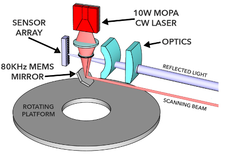
How do we achieve this? We use an unmodulated CW (constant- or continuous-wave) laser, but our MEMS mirror scans it so fast that each pixel of the sensor is illuminated for only a few nanoseconds. The sensor is a 1D array of 512 pixels, arranged vertically, and the scan is also vertical, so each scan line traverses all 512 pixels, giving us 512 data points. The mirror oscillates at ~80 kHz, and each mirror cycle consists of two lines: upward and downward. So, 80 kHz × 2 lines/cycle × 512 samples/line = 82 MSPS.
Fundamentally, this is a classic ToF lidar, with the sensor time-stamping the arrival of the reflected pulse, except that the pulse in our case is not a short burst of radiation emitted from the laser, but rather a short moment when the scanned CW laser beam is pointed in the direction of a given pixel—that’s what we call mechanical modulation. The mirror oscillations are very tightly controlled, so that time of departure is known for every sensor pixel with sub-nanosecond accuracy.
The scanner and the sensor with collection optics are placed on a rotating platform, given us a 360° horizontal FoV, or may be together bounced off another slow scan mirror, for a front-facing system. It is also conceivable to have a 2D scanner, raster-scanning a CW beam across the FoV of a 2D sensor array—our mechanical modulation would still work, but we don’t believe this would be an advantageous approach for a variety of technical reasons.
The very possibility of using a CW laser instead of a pulsed one is the main advantage of the mechanical modulation: generally, CW lasers are considerably less expensive and more efficient than their pulsed counterparts, and this is applicable to all classes of lasers: semi-conductor, solid-state, fiber, VCSEL arrays, etc. A pulsed laser is a device which is idle 99 per cent of the time. On the other hand, when it is not idle, it works extremely hard, at very high-power density levels, leading to various losses, as well as design complications.
We opted to use a semiconductor MOPA (Master Oscillator-Power Amplifier) laser, which is fundamentally a large-area edge emitter, comparable in cost and efficiency to large multi-mode laser diodes but producing a single-mode beam which is needed for scanning. However, to match the average output of a CW laser diode, perhaps dozens of pulsed ones would be needed, each costing roughly the same as our single one. Speaking of efficiency: the main source of losses in a semiconductor laser is ohmic resistance, and the power dissipation in a resistor grows as a square of the current, and therefore, is inversely proportional to the duty cycle of a pulsed laser.
Our scanned CW laser very considerably lowers the cost of each collected data point, in terms of both dollars and joules of energy, thus uniquely enabling ultra-high resolution at low cost. Another cost advantage is in the sensor: since we only need a 1D array, it is only a narrow sliver of the wafer—a fraction of a millimeter in width, occupying only a few square millimeters of the wafer area, and sensors are typically priced per wafer area.
Additionally, it turns out 1D scanners with 1D sensors convey some unique optical advantages, which allow us to simultaneously see targets very far away and very close-by.
DVN: What made your company decide to go for automotive lidar applications?

DY : As businesspeople, we surely couldn’t miss the enormous size of automotive market. On the other hand, as engineers, we see that our solution fits the automotive requirements very well: high resolution, long range and low cost. So, going after the automotive applications was a no-brainer. Having said that, we believe other applications might benefit from our lidar technology too, and we’re looking at those, but still automotive remains our focus.
As I said, the key components—MEMS mirror, MOPA laser, and 1D sensor array—have been designed, fabricated, and tested, we’ve completed system testing, and have confirmed the expected performance.
DVN: Which wavelength have you chosen, and why?
DY: We presently work with 1,550-nm lasers and linear-mode InGaAs APD sensors. However, fundamentally we’re sensor-agnostic and our system can work with any type of ToF-capable sensors at any wavelength. Our initial choice of 1,550-nm was mostly dictated by two considerations: first, we didn’t have to worry about eye safety, and second, we could easily afford the relatively high cost of InGaAs, because of our small wafer area.
However, we believe that even at 905 nm we can stay within Class 1 while emitting several watts of laser power, and that should be sufficient to reach 200 m range with advanced silicon sensors. We’re presently working in this direction. Another potentially interesting area, where our mechanical modulation may turn out advantageous, is time-domain coherent detection. By virtue of being continuously on, a CW laser of sufficiently narrow optical bandwidth becomes an ideal local oscillator for various time-domain coherent detection schemes. If successful, it might lead to considerable improvements in sensitivity, solar immunity, and interference robustness of future lidars. We’ve filed IP on this approach.
DVN : What about power consumption?
DY : Lots of data points means lots of laser power, and then lots of electric power, too. In our system, the laser dominates the power consumption, and for 1,550-nm system with a 10-watt CW laser and required cooling, the total can reach ~90W. A 905-nm system with 3W of laser power would be at ~25W.
DVN: How does your technology do in bad weather?
DY : Fundamentally our technology is subject to the same limitations in bad weather as other ToF lidars. However, in some situations we may be able to substitute quantity for quality: due to the sheer density of our point cloud, we might be able to present some meaningful information, even if, say, 90 per cent of the data points are lost. Still, there is no chance we’ll see anything 200 m away in heavy rain or fog.
DVN: When do you expect to launch your first projects on production vehicles for use on public roads?
DY : This is not up to us. At this point, we have just lidar hardware, while a lot more is needed for any public-road project. We hope our road-grade hardware can be ready within two years if everything goes well, but the decisions about any public road projects will be in the hands of our industry partners.
DVN: How do you see the automotive lidar market evolving over the next five years?
DY : I won’t speak of regional markets as I don’t know enough about their specifics, but I believe L3 vehicles will be the biggest market for lidars in the next five years. My gut feeling is that L4 might become a ‘lost generation’, as L5 robotaxis and trucks and delivery robots overtake the lidar market from high-end L4 cars in private ownership, but this will probably happen more than five years from now.
